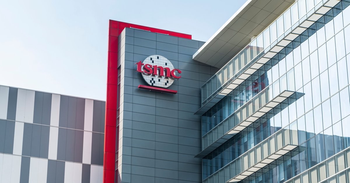
According to manufacturingdigital.com, Taiwan Semiconductor Manufacturing Company (TSMC) has pledged an additional $100 billion to expand its semiconductor campus in Arizona, bringing its total committed investment in the site to $265 billion.
TSMC’s expanded Arizona footprint
The new investment will fund the construction of four additional semiconductor fabrication facilities — or fabs — at TSMC’s Arizona site. This follows an earlier commitment under the Biden administration to build three greenfield fabs as part of a $65 billion investment. The March 2025 pledge — made after Donald Trump returned to the White House in January 2025 — also includes plans for a research and development center and two advanced packaging facilities.
The expansion is designed to meet multi-year demand from major U.S. customers and strengthen domestic semiconductor supply chains. As of mid-2026, the Arizona site has already created more than 6,000 jobs. U.S. Commerce Secretary Howard Lutnick stated the latest investment will generate “tens of thousands” of additional jobs — a figure consistent with industry benchmarks for large-scale fab builds requiring extensive construction, operations, and engineering staffing.
U.S. government support and incentives
Federal and state-level financial mechanisms significantly underpin TSMC’s decision. In 2024, the U.S. government awarded TSMC up to $6.6 billion in direct funding and up to $5 billion in potential loans under the CHIPS and Science Act. These funds are tied to specific milestones including job creation, technology transfer, and domestic production targets.
Arizona offers layered fiscal advantages: the Advanced Manufacturing Investment Credit covers up to 25% of qualified capital expenditures; the Qualified Facility Tax Credit applies to new full-time positions; and R&D expenses qualify for a 24% tax credit on the first $2.5 million, then 15% beyond that. Crucially, machinery and equipment used in manufacturing are exempt from state sales tax — a critical benefit given that a single extreme ultraviolet lithography machine costs over $200 million.
Strategic location rationale
Beyond financial incentives, Arizona provides operational stability and infrastructure readiness. Its Foreign Trade Zone designation allows TSMC to reclassify property as Class 6, slashing the property tax assessment ratio from 17% to 5%. This directly lowers long-term infrastructure ownership costs. The site also benefits from proximity to skilled engineering talent pools, reliable power infrastructure, and water management systems engineered for high-purity industrial use — all prerequisites for advanced node semiconductor manufacturing.
The timing aligns with broader geopolitical shifts: in January 2026, the U.S. and Taiwan signed a trade and investment deal reducing tariffs on Taiwanese products to 15%. This bilateral agreement supports ongoing technology collaboration while reinforcing supply chain diversification away from concentrated Asia-Pacific manufacturing hubs.
“This is to support the strong multi-year demand from our leading US customers, and we believe this investment will further foster the development of the US semiconductor ecosystem, strengthen the supply chain and support significant job creation in the United States.” — C.C. Wei, Chairman and Chief Executive Officer of TSMC
Industry analysts note that TSMC’s Arizona strategy reflects a broader trend among global foundries: Intel is investing $20 billion in Ohio and $10 billion in Arizona; Samsung recently broke ground on a $17 billion fab in Texas. Collectively, these projects represent the largest coordinated push to rebuild U.S. advanced logic manufacturing capacity since the 1980s — with implications for national security, export control compliance, and long-term R&D sovereignty.
Source: manufacturingdigital.com
Compiled from international media by the SCI.AI editorial team.