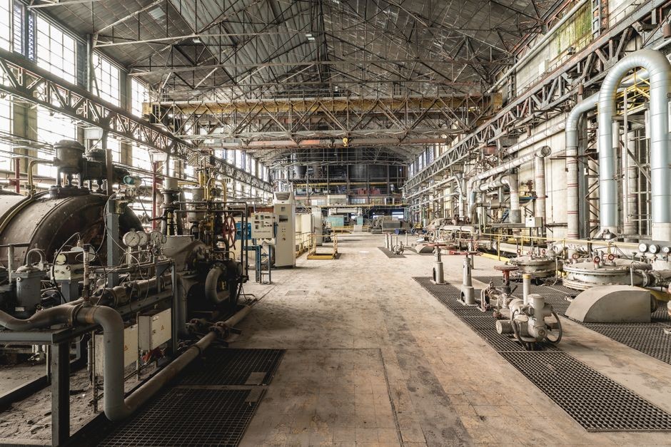
According to finance.biggo.com, Intel’s 18A process has achieved a major yield breakthrough, reaching 30,000 wafers per month across its Fab 52 in Phoenix, Arizona, and D1X facility in Hillsboro, Oregon — sufficient to meet current internal demand but requiring expansion for external foundry orders.
18A Yield Resolution and Capacity Milestones
A report from investment research firm BlueFin Research Partners confirms that yield issues with Intel’s 18A process have been resolved, marking a sharp improvement over Morgan Stanley’s May assessment — which estimated yields at only 50%. The enhanced 18A-P variant has now entered risk production at the D1X facility. This iteration delivers 9% higher performance at identical power consumption or 18% lower power at equivalent performance.
Intel’s internal production in Q2 advanced according to plan, with output rising 2% quarter-over-quarter. A further sequential increase of 1%–2% is projected for Q3. Meanwhile, equipment installation at Fab 42 in Arizona — dedicated to the Intel 7 process — is 50% complete and expected to add 7,500 wafers per month upon completion.
Advanced Process Roadmap and Foundry Strategy
Intel has initiated risk production of 18A-P at D1X and plans long-term mass production at Fab 62, with the first Ohio fab slated as the second 14A production base. The 14A process is on track: early sample tests are positive, risk production is scheduled for 2028, and large-scale mass production is targeted for 2029.
Intel CEO Lip-Bu Tan stated in May that the company expects to secure formal cooperation commitments from multiple foundry customers in the second half of 2026. Its external foundry business will prioritize advanced nodes including 18A-P, 18A-PT, and 14A. Additionally, Intel’s EMIB advanced packaging capacity is set to reach 10,000 wafers per month in Q4, and the Malaysia facility expansion plan will be announced in early 2027.
Apple’s A20 Chip and Dual-Foundry Rumors
Supply chain sources cited by technology media outlet Wccftech suggest that Apple’s A20 chip — intended for the standard iPhone 18, scheduled for launch in Q1 2027 — may partially adopt Intel’s 18A process. This would break TSMC’s longstanding monopoly on Apple’s main SoC foundry services.
The rationale centers on constrained capacity: TSMC’s 3nm node is already under intense pressure from AI-related demand, and bottlenecks are expected to extend into its 2nm node. To mitigate supply risk, Apple may accelerate adoption of a dual-foundry strategy. However, the allocation ratio remains unspecified, and the high-end A20 Pro chip is still expected to be exclusively mass-produced by TSMC barring unforeseen developments.
Wccftech notes that Intel’s 18A yield had already surpassed 55% last year and is projected to improve significantly by July 2026, strengthening its viability as a secondary supplier.
Competitive Implications and Market Context
Intel’s 18A process is positioned as a direct competitor to TSMC’s 2nm node. Securing even partial A20 orders would represent a watershed moment for Intel Foundry Services — especially given that its current 30,000 wafers/month capacity is insufficient for full-volume iPhone chip production. Future scale hinges on Fab 62 and the Ohio facilities.
While TSMC retains leadership in 2nm technology and will likely retain sole responsibility for A20 Pro, Apple’s potential shift introduces meaningful competitive pressure. Institutional investors observe that this reflects a broader industry trend: customers increasingly diversify foundry partnerships amid surging demand for sub-3nm processes. As BlueFin Research Partners emphasized, “Yield stability and capacity scalability are now validated — the question shifts from technical feasibility to commercial execution.”
Source: finance.biggo.com
Compiled from international media by the SCI.AI editorial team.