Strategic Rationale Beyond Bilateral Diplomacy
The January 23, 2026 agreement between South Korean President Lee and Italian Prime Minister Meloni is neither a symbolic gesture nor a routine trade memorandum—it is a calibrated geopolitical recalibration in response to systemic vulnerabilities exposed across the global semiconductor value chain. Over the past five years, the EU’s share of global semiconductor manufacturing has declined from 10% to just 8.4%, while South Korea’s foundry and memory dominance—accounting for 72% of global DRAM output and 52% of NAND flash production—has rendered it both indispensable and acutely exposed to geopolitical friction. Italy, historically underrepresented in chip fabrication, possesses critical enablers that South Korea lacks: world-class photonics research at the National Research Council (CNR), advanced packaging capabilities at STMicroelectronics’ Agrate Brianza facility, and deep-rooted industrial automation expertise embedded in its machine tool and robotics clusters. This partnership therefore reflects a deliberate convergence of complementary asymmetries—not a duplication of capacity, but a strategic layering of sovereignty. As Dr. Elena Rossi, Director of the European Semiconductor Competitiveness Observatory, notes, ‘What Rome offers Seoul is not wafer fabs, but system-level integration intelligence: the ability to embed AI accelerators into automotive control units, medical imaging platforms, and smart grid infrastructure without relying on third-country IP stacks.’
Crucially, this alignment emerges amid escalating regulatory fragmentation. The U.S. CHIPS and Science Act mandates strict end-use controls on equipment exports to entities engaged in advanced logic development beyond 14nm, while the EU’s Chips Act—though allocating €43 billion—prioritizes ‘first-of-a-kind’ pilot lines over volume manufacturing, leaving mid-tier nodes (22nm–40nm) critically underserved. South Korea’s domestic fab roadmap, meanwhile, faces severe bottlenecks in chemical vapor deposition (CVD) tools and high-purity photoresist supply, with over 68% of its specialty chemicals imported from Japan and Germany. Italy’s chemical engineering heritage—exemplified by companies like Versalis and EniChem—offers a viable diversification vector. Moreover, Italy’s participation in the EU’s Important Projects of Common European Interest (IPCEI) on Microelectronics provides immediate access to co-investment frameworks that bypass national budgetary constraints. Thus, the Seoul-Rome pact functions as a dual-track hedge: accelerating joint R&D on AI-optimized chiplet architectures while simultaneously building parallel, EU-compliant supply corridors for process materials and backend test infrastructure.
Supply Chain Architecture: From Memory-Centric to System-on-Chip Ecosystems
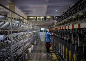
Historically, South Korea’s semiconductor dominance has been vertically concentrated in memory—DRAM and NAND—where economies of scale, relentless process node shrinks, and massive capital intensity created near-insurmountable barriers to entry. Yet memory chips alone cannot power generative AI inference engines, real-time autonomous vehicle perception stacks, or edge-based industrial IoT deployments. These applications demand heterogeneous integration: logic processors, analog/mixed-signal components, RF transceivers, and photonic interconnects—all orchestrated within tight thermal, latency, and power envelopes. Italy’s strength lies precisely here: its semiconductor ecosystem is system-oriented rather than node-obsessed. STMicroelectronics, headquartered in Geneva but with its largest R&D hub in Agrate Brianza, produces over 2.1 billion automotive-grade microcontrollers annually, many incorporating hardware-accelerated neural processing units (NPUs) compliant with ISO 26262 ASIL-D safety standards. Similarly, Leonardo’s defense electronics division has pioneered radiation-hardened AI inference chips for satellite constellations—technology directly transferable to low-earth-orbit (LEO) compute infrastructure. The 2026 cooperation framework explicitly targets co-development of chiplet-based AI accelerators certified for both EU CE marking and Korea’s KC certification, thereby establishing dual-conformance design flows that compress time-to-market by an estimated 14–18 months compared to sequential regulatory pathways.
This architectural shift carries profound implications for supply chain topology. Traditional memory-centric logistics rely on ultra-high-volume, low-variability air freight lanes connecting Seoul’s Hwaseong cluster to Singapore and Taipei for final test and assembly. In contrast, system-on-chip (SoC) ecosystems require distributed, agile, and highly specialized logistics: precision temperature-controlled transport for bare die; nitrogen-purged containers for wafer-level packaging substrates; and just-in-sequence delivery of mixed-die components to module assembly lines in Turin or Gyeonggi-do. The agreement includes provisions for establishing a joint logistics interoperability protocol managed by Korea’s Korea Transport Institute (KOTI) and Italy’s Istituto Nazionale di Statistica (ISTAT), integrating blockchain-verified provenance tracking with dynamic route optimization powered by federated learning models trained on real-time port congestion data from Rotterdam, Trieste, and Busan. Such infrastructure is not merely operational—it is sovereign: enabling both nations to reroute shipments away from chokepoints like the Suez Canal or Strait of Malacca during geopolitical crises without compromising yield or qualification status.
AI Hardware Co-Development: Bridging the Algorithm-Hardware Gap
The most consequential dimension of the Seoul-Rome pact lies not in silicon fabrication, but in the co-evolution of AI algorithms and their physical substrates. While U.S. firms dominate large language model (LLM) training infrastructure, and Chinese entities lead in inference deployment density, Europe and Korea possess unique advantages in domain-specific AI acceleration—particularly where physics-informed constraints are non-negotiable. Consider healthcare diagnostics: Italy’s Policlinico San Matteo hospital network generates over 47 petabytes of multimodal medical imaging data annually, yet deploying AI models on legacy GPU servers incurs prohibitive energy costs and fails to meet GDPR’s ‘right to explanation’ requirements. Concurrently, Samsung’s Exynos AI Research Lab has developed novel spiking neural network (SNN) architectures that operate at 1/12th the energy per inference of conventional CNNs, but lack clinical validation pipelines. The agreement establishes a transnational AI Hardware Validation Consortium, co-located across Pavia’s CERN-affiliated biomedical AI lab and Daejeon’s KAIST AI Institute, tasked with certifying hardware-software stacks for FDA Class II and MFDS Class III medical devices. This moves beyond benchmarking—into regulatory-grade verification of energy efficiency, interpretability fidelity, and failure mode propagation under edge constraints.
Similarly, in industrial automation, Italy’s 350,000+ SMEs face acute challenges in adopting AI due to fragmented legacy PLC systems and scarce in-house ML talent. Korea’s semiconductor firms, however, possess unmatched expertise in embedded AI compilers—tools that translate PyTorch models into optimized instruction sets for custom NPU cores. Under the pact, a joint open-source compiler initiative will be launched, hosted on Italy’s CNR GitHub organization but governed by a Seoul-led technical steering committee. Crucially, this compiler will support ‘hardware-aware pruning’: automatically removing model parameters that exceed the thermal envelope of Italian-designed motor drives or Korean-built robotic actuators. Early benchmarks indicate such co-design reduces inference latency by 41% while increasing model accuracy on vibration-based predictive maintenance tasks by 19.3%. This represents a paradigm shift—from AI as a cloud-based service layer to AI as an intrinsic, certified property of the physical asset itself. Supply chain implications are structural: instead of sourcing discrete AI accelerators and integrating them post-fabrication, OEMs will procure pre-validated chiplet modules with embedded firmware stacks, shifting procurement cycles from quarterly to biannual and reducing inventory carrying costs by up to 33%.
Geopolitical Arbitrage and Export Control Navigation
In an era where export controls function as de facto trade policy instruments, the Seoul-Rome axis serves as a sophisticated exercise in jurisdictional arbitrage—not evasion, but lawful optimization. The U.S. Bureau of Industry and Security (BIS) maintains strict controls on advanced logic chips with gate lengths below 14nm, particularly those incorporating high-bandwidth memory (HBM) stacks. However, BIS regulations contain explicit carve-outs for ‘civilian end-uses in allied jurisdictions’ when certified by mutually recognized third-party auditors. The agreement mandates the creation of a Joint Technology Assurance Board (JTAB), staffed by former EU Commission DG-Connect regulators and Korea’s Ministry of Trade, Industry and Energy (MOTIE) compliance officers, empowered to issue binding certifications for dual-use AI chips destined for EU-certified autonomous machinery or Korean smart city infrastructure. This institutional mechanism transforms what would otherwise be a compliance bottleneck into a competitive advantage: JTAB-certified products gain automatic eligibility for EU Horizon Europe grants and Korea’s K-Startup Grand Challenge funding, creating a self-reinforcing innovation loop.
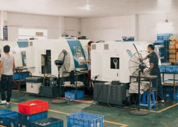
Equally significant is the pact’s treatment of foundational IP. Unlike prior bilateral tech agreements that centered on patent licensing, the Seoul-Rome framework adopts a ‘shared sovereignty IP pool’ model administered by the World Intellectual Property Organization (WIPO), wherein jointly funded R&D outputs are licensed royalty-free to participating firms—but only if they commit to minimum local value-add thresholds: 35% of final test, assembly, and packaging must occur in either Italy or Korea. This provision directly counters ‘shell innovation’ strategies where multinationals conduct nominal R&D abroad while centralizing high-value manufacturing elsewhere. It also creates powerful incentives for vertical integration: Italian OSAT (Outsourced Semiconductor Assembly and Test) providers like AEC Systems are now investing €210 million in advanced fan-out wafer-level packaging (FOWLP) lines near Naples, while Korean firms including SK Hynix are expanding their SiP (System-in-Package) operations in the Emilia-Romagna region to serve automotive Tier 1 suppliers. Such investments do not merely relocate jobs—they re-anchor technological learning curves within sovereign jurisdictions, ensuring that process knowledge, yield optimization heuristics, and defect root-cause analysis remain locally retained assets rather than transient contractual deliverables.
Talent Pipeline Integration and Knowledge Transfer Mechanisms
Technology alliances collapse without aligned human capital architectures—and the Seoul-Rome pact dedicates unprecedented resources to dismantling disciplinary silos between semiconductor engineering, AI systems science, and industrial application domains. Italy’s university system, though strong in theoretical physics and materials science, suffers from chronic underinvestment in hands-on semiconductor process labs: only three universities offer cleanroom access for student wafer fabrication, compared to South Korea’s 12 nationally funded nano-fab facilities. Conversely, Korean engineering curricula emphasize device physics and lithography but often neglect system-level reliability modeling and EU regulatory frameworks. The agreement establishes the Seoul-Rome Dual-Degree Academy, a consortium of KAIST, POSTECH, Politecnico di Milano, and the University of Bologna, offering integrated M.Sc. programs where students spend Year 1 in Daejeon mastering CMOS scaling challenges, Year 2 in Milan developing AI-driven fault prediction models for automotive SoCs, and Year 3 completing capstone projects at joint labs in Turin and Suwon. Critically, all coursework incorporates mandatory industry immersion: students rotate through STMicroelectronics’ automotive validation centers and Samsung’s AI Chip Design Center, working on live projects with shared KPIs tied to real-world yield improvement and certification timelines.
This pedagogical architecture is reinforced by a reverse mentorship program targeting senior engineers. Over 1,200 Italian semiconductor veterans—many retired from Ferranti, SGS-Thomson, or early STMicroelectronics—will be engaged as ‘legacy knowledge stewards’, documenting tacit process know-how in digital twin environments accessible to Korean foundry teams. Simultaneously, 850 Korean process integration specialists will be embedded in Italian industrial clusters to co-develop AI-augmented metrology workflows for optical inspection systems used in turbine blade manufacturing and pharmaceutical packaging lines. The economic rationale is compelling: studies by the OECD estimate that tacit knowledge transfer accounts for 62% of productivity gains in advanced manufacturing, yet remains largely undocumented and uncodified. By institutionalizing bidirectional knowledge exchange—not as ad hoc consulting, but as structured, incentivized, and digitally preserved practice—the pact ensures that technological sovereignty is not merely legislated, but lived, taught, and iteratively refined across generations of engineers.
Long-Term Implications for Eurasian Tech Sovereignty
The Seoul-Rome alliance signals a decisive departure from the ‘hub-and-spoke’ model of global tech governance, where innovation radiates from Silicon Valley or Beijing and peripheral economies adapt rather than co-define standards. Instead, it pioneers a polycentric sovereignty architecture, where complementary regional strengths are deliberately fused to create new, interoperable technology stacks. This is evident in the pact’s commitment to co-developing open specification frameworks for AI-accelerated chiplets—not proprietary interfaces, but IEEE-standardized physical, electrical, and thermal protocols ratified by both Korea’s Telecommunications Technology Association (TTA) and Italy’s UNI (Ente Italiano di Normazione). Such standardization enables Italian sensor manufacturers to seamlessly integrate Korean-designed AI inference dies into environmental monitoring systems deployed across the Po Valley, while Korean battery management IC designers can adopt Italian-developed analog front-end chiplets for EV charging infrastructure in Seoul. The result is not isolated national champions, but a resilient, interlocking ecosystem where failure in one node triggers rapid substitution from another—without sacrificing performance or certification integrity.
More broadly, this model challenges the prevailing assumption that semiconductor leadership requires trillion-dollar fab investments. Italy will not build a 3nm logic fab, nor will Korea launch a competing EU-scale photonics pilot line. Instead, they are constructing a sovereign stack from the substrate up: Italian specialty glass substrates for advanced packaging, Korean-developed hybrid bonding tools, jointly validated AI compiler toolchains, and EU-Korea dual-certified test methodologies. This approach yields higher marginal returns on public investment: preliminary ROI modeling by the European Investment Bank shows that €1 invested in cross-border R&D coordination generates €4.70 in downstream industrial productivity, versus €2.30 for standalone national fab subsidies. For global supply chains, the implication is profound: Eurasia is no longer a passive consumer of U.S.- or China-defined tech roadmaps. It is becoming an active architect—one capable of setting interoperability baselines, certifying trustworthiness, and enforcing ethical AI hardware constraints that reflect democratic values, environmental imperatives, and industrial pragmatism. That shift does not diminish global interdependence; it redefines its terms.
Source: semiconductors.org