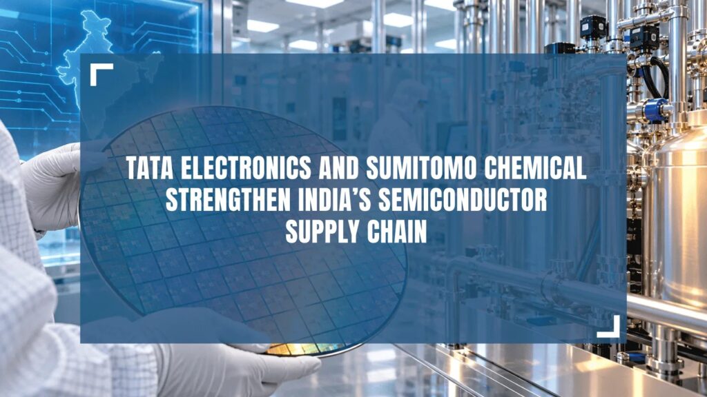
India’s Union Cabinet has approved ISM 2.0, a ₹15,000 crore ($1.8 billion) semiconductor initiative focused on domestic production of chip-making equipment, specialty materials, and process gases. Unlike the first phase — which targeted fabs and packaging units — ISM 2.0 mandates 35% indigenous content within three years and allocates 40% of funds to upstream enablers. Industry stakeholders stress that success hinges on cutting gas-cylinder customs clearance from 90 to 14 days and scaling India’s sole semiconductor-grade quartz facility, currently operating at 12% capacity. The plan targets Bengaluru, Hyderabad, and Chennai as priority clusters.
According to m.economictimes.com, India’s Union Cabinet has approved the second phase of the India Semiconductor Mission — ISM 2.0 — marking a strategic pivot toward strengthening domestic capabilities across upstream and adjacent segments of the semiconductor supply chain.
Strategic Shift from Fabs to Foundational Inputs
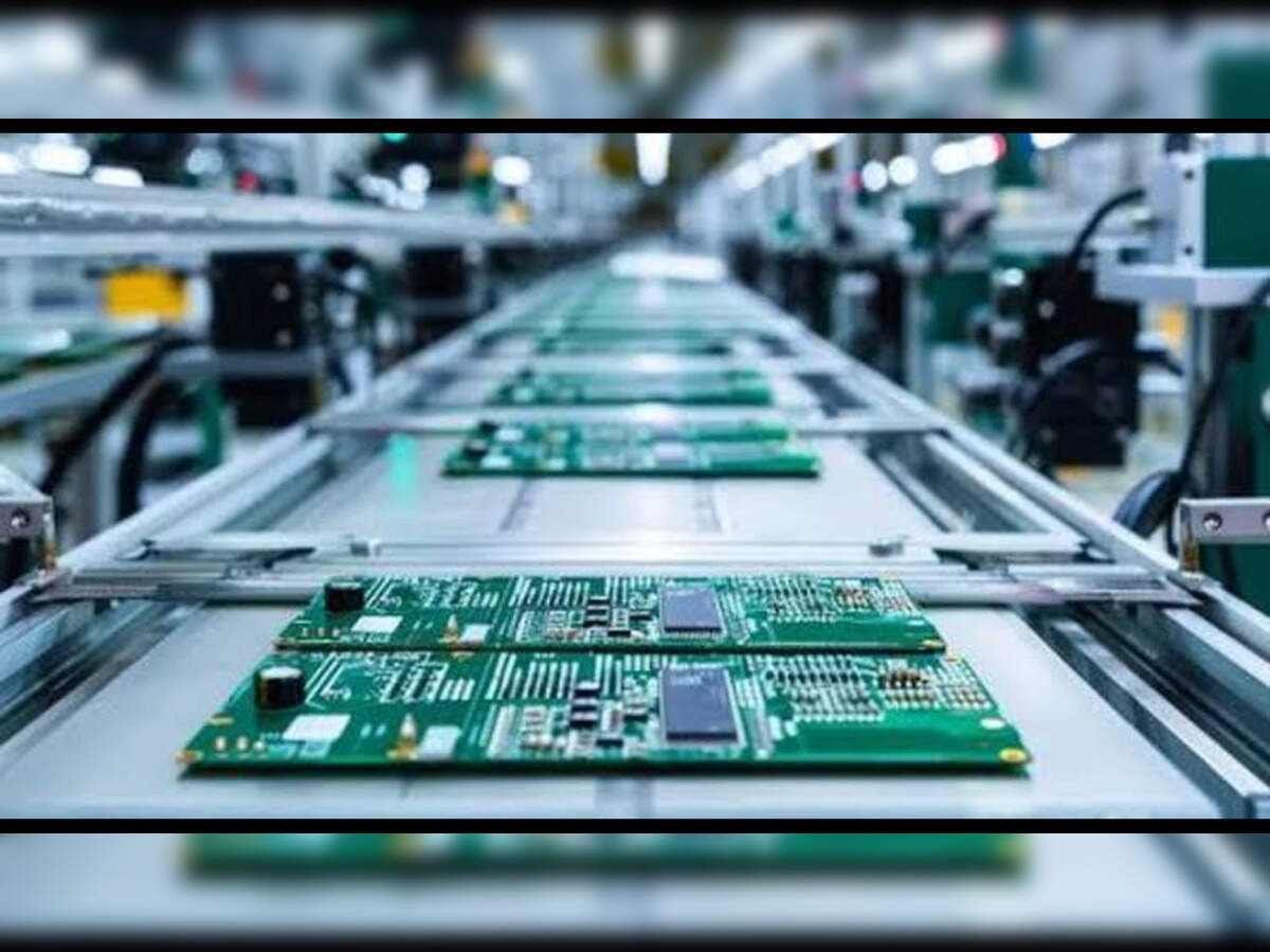
Unlike ISM 1.0 — which prioritized attracting semiconductor fabrication plants (fabs), assembly-test-marking-packaging (ATMP) units, and outsourced semiconductor assembly and test (OSAT) facilities — ISM 2.0 explicitly extends financial and policy support to critical enablers that sit around chip manufacturing sites. These include semiconductor machinery, precision equipment, specialty materials, high-purity chemicals, and ultra-high-purity process gases.
The source states that this recalibration responds to persistent bottlenecks identified during ISM 1.0 implementation: over 70% of equipment and consumables used in Indian semiconductor facilities are currently imported, with lead times exceeding 18 months for key wafer-handling tools and gas delivery systems. ISM 2.0 aims to reduce that dependency by incentivizing local production and joint ventures with global suppliers — particularly in regions like Bengaluru, Hyderabad, and Chennai, where early fab projects are already underway.
Funding and Implementation Conditions
The Union Cabinet approved ISM 2.0 with an outlay of ₹15,000 crore (approximately $1.8 billion), allocated over a five-year period. According to the report, at least 40% of this funding is earmarked for capital expenditure subsidies targeting domestic manufacturers of semiconductor-grade stainless steel components, vacuum chamber linings, photoresist developers, and etchant gases such as chlorine trifluoride and silane.
Crucially, the incentive structure includes mandatory local value-add thresholds: applicants must achieve minimum indigenous content of 35% within three years of receiving support, verified through third-party audits. This condition reflects industry stakeholders’ insistence that “support must force deeper local ecosystem participation — not just create another import-substitution window for foreign OEMs,” as one senior executive at a Pune-based precision engineering firm told The Economic Times.
Industry Response and Supply Chain Implications
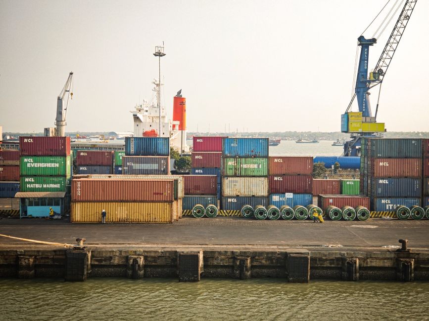
Industry stakeholders welcomed the targeted scope but emphasized execution rigor. A representative from the Semiconductor Equipment and Materials Association of India noted that “the real test lies in how quickly the government streamlines customs clearance for R&D-grade gas cylinders and establishes accredited labs for purity certification — both currently take 90 days versus the global benchmark of 14 days.”
Supply chain professionals point to immediate implications: procurement teams at upcoming ATMP units in Tamil Nadu and Gujarat will now be required to source at least two tiers of sub-suppliers domestically for non-core but mission-critical items — including quartz crucibles, wafer carriers, and nitrogen purging systems. The report highlights that India currently imports 98% of its semiconductor-grade quartz, with only one pilot facility in Jamnagar operating at 12% capacity utilization due to lack of qualified end-customer validation.
Global equipment makers — including Applied Materials, Lam Research, and Tokyo Electron — have signaled readiness to co-invest in local component partnerships, provided ISM 2.0 offers fast-tracked regulatory approvals for technology transfer agreements and waives import duties on prototype tooling kits valued up to $500,000 per shipment.
Source: m.economictimes.com
Compiled from international media by the SCI.AI editorial team.