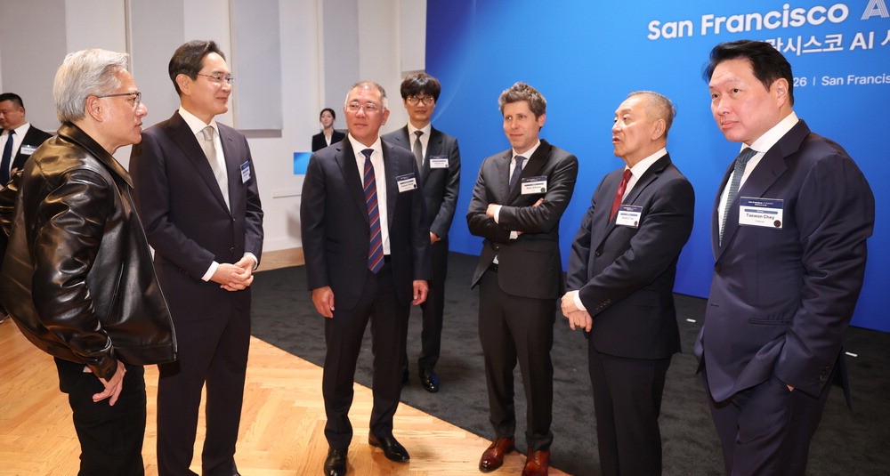
According to pulse.mk.co.kr, Samsung Electronics Co. and U.S. chip designer Broadcom Inc. have formed a strategic partnership valued at $200 billion to build an integrated, one-stop artificial intelligence (AI) semiconductor supply chain through 2030.
Partnership Signed at San Francisco AI Summit
The two companies signed a memorandum of understanding (MOU) at the San Francisco AI Summit — an event organized by the Korean government and held in San Francisco on Friday, July 27, 2026. Under the agreement, Samsung will deliver a fully integrated supply solution to Broadcom, combining its HBM4 and HBM4E high-bandwidth memory chips, sub-2-nanometer foundry process technology, and advanced packaging capabilities — all tailored for next-generation AI accelerators and high-speed networking chips.
The collaboration spans three core domains: memory, foundry manufacturing, and advanced packaging — with plans to expand across all three over the next five years. This marks a structural shift from traditional GPU-centric AI infrastructure toward custom application-specific integrated circuits (ASICs), a trend increasingly adopted by major technology firms.
Broadcom’s Rapid AI Chip Revenue Growth
Broadcom’s AI semiconductor revenue reached $10.8 billion in the second quarter of fiscal 2026, representing a 143 percent year-on-year increase. Industry projections indicate that figure will climb to $16 billion in the third quarter — underscoring surging demand for custom AI accelerators and AI-optimized networking chips.
Analysts note this growth is intensifying pressure on manufacturing partners capable of delivering tightly integrated solutions — particularly those that can co-package memory, compute logic, and interconnect technologies within a single platform. “The partnership lays the groundwork for Samsung to become an integrated AI semiconductor provider spanning memory and foundry, though its success will depend on customer qualification, 2-nanometer yields, advanced packaging capacity and final order volumes,” said an industry official.
Strategic Benefits for Samsung
The deal offers Samsung multiple strategic advantages. Diversifying its high-bandwidth memory (HBM) customer base could reduce reliance on any single client — a key risk given current concentration among top AI hardware vendors. Successfully mass-producing sub-2-nanometer chips for Broadcom would serve as critical validation of Samsung’s manufacturing yields and process reliability — potentially unlocking additional foundry orders from other global clients.
Bundling memory, foundry services, and advanced packaging into a single commercial offering is expected to deepen customer relationships beyond transactional product sales. Closer engineering collaboration may also shorten development cycles and lower power consumption in end-system designs — both vital metrics for AI datacenter deployments.
Geopolitical and Supply Chain Implications
The partnership has fueled expectations that Samsung could emerge as a viable alternative to Taiwan Semiconductor Manufacturing Co. (TSMC) in the advanced foundry and packaging ecosystem — particularly in the AI accelerator market, where HBM integration and 2.5D/3D packaging are now decisive performance factors.
By enabling tighter integration between memory and logic die, Samsung’s full-stack capability could help ease manufacturing bottlenecks, reduce geographic concentration in the AI chip supply chain, and improve price and delivery competitiveness for global cloud and infrastructure providers. The initiative aligns with broader Korean government efforts to strengthen domestic semiconductor sovereignty — including recent diplomatic outreach culminating in the San Francisco summit, where Korean President Lee met with U.S. AI executives as part of a planned $950 billion AI mega-alliance.
Source: pulse.mk.co.kr
Compiled from international media by the SCI.AI editorial team.