According to www.bisinfotech.com, the global semiconductor supply chain is uniquely fragile — a single chip crosses international borders up to 70 times before reaching end users, and Taiwan Semiconductor Manufacturing Company (TSMC) commands nearly 70% of the global foundry market share for advanced chips.
Structural Complexity and Revenue Scale
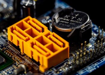
The microchip underpins modern economic infrastructure — from smartphones to automotive systems — with global chip revenue nearing $820 billion. Yet this explosive growth has exposed deep structural vulnerabilities. Unlike conventional manufacturing concentrated in one location, semiconductor production spans multiple continents and relies on highly specialised intellectual property, extreme precision, and tightly coordinated handoffs among geographically dispersed entities.
The value chain begins with Electronic Design Automation (EDA) software and intellectual property (IP) cores — dominated by firms in North America and Europe. Designing a sophisticated microchip involves placing billions of transistors onto silicon wafers smaller than a fingernail, using software that ensures thermal stability and functional integrity. This upstream stage sets the technical foundation for all downstream fabrication and packaging.
Midstream: Wafer Fabrication and Capital Intensity
After design, “fabless” companies like Nvidia, AMD, and Qualcomm outsource production to wafer foundries — the most capital-intensive segment of the value chain. These ultra-clean fabrication facilities use photolithography techniques to layer materials onto silicon wafers. The process demands multi-billion-dollar investments and years of lead time: building new fabs is slow, expensive, and technically demanding.
As of July 6, 2026, government initiatives such as the U.S. CHIPS and Science Act, the European Chips Act, and India’s expanded Semiconductor Mission (ISM 2.0) — which recently secured a multi-billion dollar budgetary approval — aim to re-shore production and diversify geographic concentration. However, these efforts cannot resolve supply chain fragility overnight due to the scale and timeline required for fab construction.
Downstream: ATP/OSAT and Labor-Intensive Final Stages
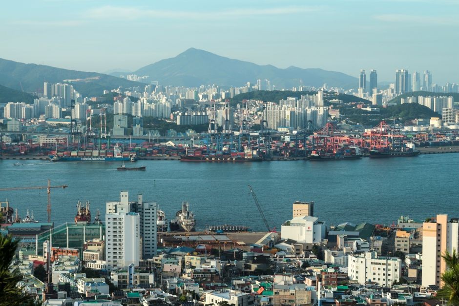
Once wafers are fabricated, they are diced into individual dies, then packaged, tested, and assembled — a phase known as Assembly, Testing, and Packaging (ATP) or Outsourced Semiconductor Assembly and Test (OSAT). This labor-intensive final step is heavily concentrated in Southeast Asia and China.
ATP represents the last physical link before chips enter circuit boards and finished devices. Its geographic clustering adds another layer of vulnerability — particularly amid rising labor costs, regulatory shifts, and logistical bottlenecks across regional ports and air freight corridors. Delays at this stage ripple backward, stalling production lines for automotive OEMs and consumer electronics brands alike.
Geopolitical Bottlenecks: Taiwan Strait Risk and Export Controls
The most acute geopolitical vulnerability lies in the Taiwan Strait: nearly 60% of the most advanced semiconductors — those powering AI infrastructure and military defense systems — are manufactured in Taiwan. That concentration exposes the global supply chain to seismic risk, drought-induced water shortages, and escalating political tensions.
Disruption to maritime traffic through the Taiwan Strait would halt electronics shipments globally within hours. Compounding this, governments have deployed aggressive export controls targeting front-end etching systems, EDA software, and Extreme Ultraviolet Lithography (EUV) machines. These restrictions — enforced since 2024 and tightened through 2026 — have the same operational impact as physical disruptions: they impede chip sales, block software distribution, and constrain logic design options in targeted foundries.
Upstream Sourcing: Rare Gases, Specialty Chemicals, and Mineral Substrates
Beyond fabrication and packaging, upstream bottlenecks pose equally severe threats. Semiconductor manufacturing requires high-purity specialty chemicals, rare gases (e.g., neon, krypton), and unique mineral substrates — many sourced from just one or two countries. Shortages of these inputs, often overlooked in public discourse, can halt entire production lines even when fabs operate at full capacity.
For example, neon gas — critical for laser-based lithography — saw prices surge 300% during the 2022–2023 supply shock triggered by conflict-related production halts in Ukraine. Similarly, fluorinated gases used in etching processes face tightening environmental regulations across the EU and Japan-Korea region, forcing rapid substitution and qualification cycles that delay ramp-up timelines by 6–12 months.
Source: bisinfotech.com
Compiled from international media by the SCI.AI editorial team.